Image Grok Imagine
Visualizing TERAFAB’s Semiconductor Innovation Through Technical Artistry
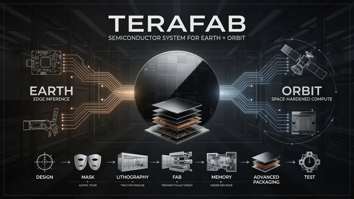
Detailed conceptual visual of TERAFAB’s semiconductor manufacturing, featuring symmetrical design and hybrid sculpture elements that emphasize chip architecture and distinct Earth and orbital deployment streams.
Prompt
{
  "subject": "TERAFAB, a proposed semiconductor complex by Tesla, SpaceX, and xAI",
  "intent": "beautiful high-end infographic grounded in semiconductor manufacturing, not a generic robot factory",
  "mode": "concept announcement visual, not a finished documentary photo",
  "canvas": {
    "aspect_ratio": "16:9",
    "resolution": "ultra",
    "background": "deep black graphite with faint cleanroom haze, subtle film grain, controlled vignette"
  },
  "headline": {
    "title": "TERAFAB",
    "subtitle": "SEMICONDUCTOR SYSTEM FOR EARTH + ORBIT",
    "placement": "center top",
    "font_style": "clean geometric sans-serif, ultra precise, Tesla-like restraint",
    "color": "#F3F4F6",
    "tracking": "wide",
    "hierarchy": "strong title, restrained subtitle"
  },
  "composition": {
    "layout": "strict symmetrical center composition with two mirrored output streams",
    "centerpiece": "one monumental silicon wafer and chip-stack diagram floating in the middle",
    "left_stream": "terrestrial inference chip path",
    "right_stream": "space-hardened chip path",
    "lower_band": "under-one-roof manufacturing stages",
    "negative_space": "generous and intentional, no clutter"
  },
  "central_visual": {
    "type": "hybrid semiconductor sculpture + technical infographic",
    "description": [
      "a large 300mm silicon wafer viewed front-on, polished dark mirror surface with fine die-map geometry",
      "a precise cross-section through the wafer revealing layered chip architecture",
      "photomask patterns, circuit traces, microscopic interconnect grids, package substrate layers, test contact points",
      "floating chip package stack beneath the wafer, beautifully aligned, clean, engineered, monumental",
      "no car assembly line, no factory robots, no generic sci-fi machinery"
    ],
    "materials": [
      "polished silicon",
      "brushed aluminum",
      "clean glass",
      "dark ceramic package surfaces",
      "fine copper interconnect accents"
    ],
    "lighting": "cold white cleanroom beams from above, sharp edge reflections, restrained glow, no neon excess"
  },
  "dual_chip_story": {
    "left_path": {
      "theme": "EARTH",
      "label": "EDGE INFERENCE",
      "visual_language": [
        "copper-gold signal flow",
        "subtle silhouettes of a vehicle control board and a humanoid hand actuator",
        "dense efficient compute, compact power envelope",
        "clean circuit routes moving from wafer to packaged chip to terrestrial deployment"
      ]
    },
    "right_path": {
      "theme": "ORBIT",
      "label": "SPACE-HARDENED COMPUTE",
      "visual_language": [
        "cold blue-white signal flow",
        "subtle satellite geometry, orbital arc lines, thermal radiator motifs",
        "high-temperature and radiation-tolerant implication without cartoon effects",
        "clean circuit routes moving from wafer to packaged chip to orbital deployment"
      ]
    }
  },
  "manufacturing_band": {
    "placement": "lower third",
    "style": "elegant linear process strip with exact spacing",
    "stages": [
      "DESIGN",
      "MASK",
      "LITHOGRAPHY",
      "FAB",
      "MEMORY",
      "ADVANCED PACKAGING",
      "TEST"
    ],
    "visuals": [
      "mask reticle geometry",
      "cleanroom corridor modules",
      "wafer carriers",
      "process chambers as abstract engineered forms",
      "metrology markers",
      "package cross-sections"
    ]
  },
  "location_and_scale": {
    "placement": "small controlled annotations",
    "elements": [
      "AUSTIN, TEXAS",
      "TWO CHIP FAMILIES",
      "TERAWATT-SCALE TARGET",
      "UNDER ONE ROOF"
    ],
    "style": "tiny monochrome microtext, highly legible, evenly spaced"
  },
  "typography": {
    "system": "single geometric sans-serif family plus minimal monospaced micro labels",
    "rules": [
      "perfect kerning",
      "high readability",
      "no warped glyphs",
      "no gibberish text",
      "clear hierarchy through size and spacing only"
    ]
  },
  "graphic_elements": {
    "connectors": "hairline technical rules, exact anchor points, no floating lines",
    "grids": "very subtle engineering grid in background",
    "micro_markers": "measurement ticks, die labels, alignment marks, tiny index numbers",
    "icons": "minimal semiconductor and orbital symbols only"
  },
  "color_palette": {
    "base": [
      "#07090B",
      "#111317",
      "#F3F4F6",
      "#9CA3AF"
    ],
    "accents": [
      "#C58B3A",
      "#7CC7FF"
    ],
    "usage": "gold-copper only for terrestrial signal path, cold blue only for orbital signal path, everything else neutral and disciplined"
  },
  "aesthetic_direction": {
    "style": "luxury industrial editorial, launch-event graphic, advanced semiconductor beauty",
    "mood": "inevitable, precise, ambitious, engineered",
    "finish": "crisp, expensive, calm, exact"
  },
  "strict_constraints": [
    "do not depict a generic autonomous megafactory",
    "do not use automotive assembly lines",
    "do not use random robot arms as the main subject",
    "do not turn it into a space colony poster",
    "do not emphasize solar farms or construction equipment",
    "do not use fake dashboard UI clutter",
    "do not overload with unreadable statistics",
    "do not make it look like a stock corporate infographic"
  ],
  "forbidden": [
    "blurry text",
    "plastic materials",
    "rainbow sci-fi lighting",
    "busy composition",
    "fantasy machinery",
    "solar-panel-dominant imagery",
    "cartoon satellites",
    "random meaningless numbers"
  ]
}
Published: April 3, 2026 by @IamEmily2050